
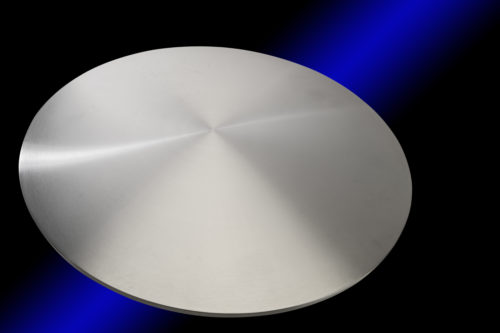
 First discovered in 1852 and developed as a thin film deposition technique in 1920, sputtering targets are a physical vapor deposition mechanism—an old process, but with many uses in modern technology and manufacturing. The process starts by feeding a substrate (or other item to be coated) into a vacuum chamber containing two magnets. After introducing a controlled gas (such as argon) into the chamber, powerful magnets pull atoms from the substrate.
These atoms then proceed to collide with each other in their gaseous state before condensing into a plasma that dries into a thin film on the substrate. The final product is a thin but durable coating valid across a variety of applications.
Applications
Many products commonly used today have a coating created through sputtering targets. These coatings include:
- Semiconductors
Most modern day electronics incorporate essential components which have been produced with tantalum sputtering targets. These include microchips, memory chips, print heads, flat panel displays as well as others.
- Glass Coating
Sputtering targets are used to produce low-radiation coated glass – also known as Low-E glass – which is commonly used in building construction because of its ability to save energy, control light, and for aesthetics.
- Solar Cell Coating
Demands for renewable energy are on the rise. Third generation, thin-film solar cells are prepared using sputter coating technology.
Available Materials from Admat
These versatile coatings each have different applications for which they are best suited. At Admat, we offer an expansive selection of material, our most common including:
- Tantalum
Used as a barrier layer on silicon wafers for semiconductor production, tantalum is used in all modern electronics. Cell phones, DVD and Blu-ray players, laptops, automobile electronics and even gaming consoles contain tantalum.
- Niobium
Commonly used in electronics, niobium has similar properties to tantalum. Niobium is corrosion resistant due to its oxide film and is a considered a superconductor.
- Titanium
Found in a wide variety of conventional products including watches, laptops, and bicycles, titanium is lightweight and corrosion resistant. This material is often used for wear-resistance and aesthetic design, but may also be used for semiconductors and optical coatings.
- Tungsten
Tungsten thin films are a decorative coating widely used for their thermal, physical, and mechanical properties such as a high melting point and thermal conductivity.
- Molybdenum
Having a lower density and consistent pricing, this element can be used in place of tungsten and is commonly used to coat solar panel cells.
- Hafnium
Hafnium films are frequently used as an insulator for semiconductors, as well as for surface hardness and protection. As an element with a high dielectric constant, it may improve the performance of some electronics.
- Silicon
This target material is most generally used in the production of silicon solar cells.
Learn More from Admat
Sputtering is a perfect way for many manufacturers to add durability and functionality to substrates and parts in a variety of applications. Contact Admat today to find out how we can assist you in selecting the appropriate materials for your coating and fabrication needs.